The Link Between Signal Integrity and Power Integrity in Your PCB

The Link Between Signal Integrity and Power Integrity in Your PCB
You can thank Bert Simonovich and Eric Bogatin for making it clear: signal integrity, power integrity, and conducted and radiated EMI cannot be considered in isolation. An issue in one area can cause a problem in another area, leading to signal degradation and instability throughout your PCB.
The primary link between signal integrity and power integrity arises at the board and chip level. When we look within a functional block in a PCB, we have a problem where power integrity in an upstream portion of the board creates a signal integrity and power integrity problem in a downstream portion. Similarly, a power integrity problem during switching in one functional block will propagate the same disturbance to all other functional blocks at the same hierarchical level. Here, we’re talking about much more than just conducted/radiated EMI from a switching regulator; this particular transient power integrity problem is intimately related to the geometry of your PCB layout. Solving these problems takes some considerable layout experience and some basic calculations before creating your layout. Let’s take a look at the important PDN design points to consider before you create your electronics schematics.
Signal Integrity and Power Integrity Effects
Power integrity problems have been discussed in a few of our other blog posts. Proper PDN design begins with your stackup, and confronting power integrity issues early will help suppress signal integrity problems that are not related to parasitics in your PCB layout. The principle of power integrity problems that need to be considered in your PCB are:
- DC voltage drop on the PDN (a.k.a. IR losses). This is effectively a parasitic effect due to the nonzero DC resistance of conductors in your PDN. There is no getting around the DC voltage drop in your PDN. As long as you are not repeatedly routing through vias and your board is manufactured properly, you can usually ignore this source of power degradation.
- Strong ripple voltage on the PDN. When components switch in your board, they draw a strong burst of current from the regulator in your board. Parasitic capacitance and inductance in your board, as well as your decoupling capacitors, cause your PDN to behave as a complicated RLC network. This causes the current impulse to produce a transient current response, which can be underdamped, critically damped, or overdamped. The voltage ripple produced by this response is equal to the current ripple multiplied by the PDN impedance. This is also a source of conducted and radiated EMI.
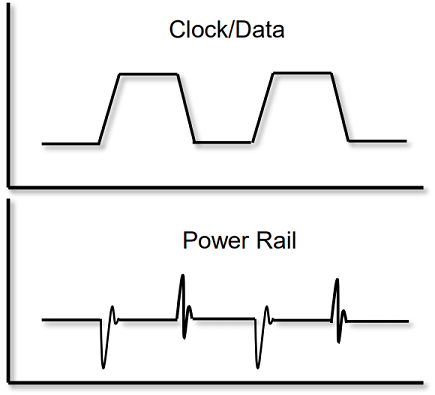
Each time an IC switches, a transient response will propagate on the PDN.
These two effects encompass the DC and AC forms of power integrity in your PCB. The DC portion is unavoidable, but it also plays a less important role than the AC portion described above. When ringing occurs on your PDN, the voltage fluctuation changes the gate-source and/or source-drain voltages seen in an IC. This causes the equivalent RC time constant at the output of the IC to fluctuate, and it causes fluctuations in the output signal level. This voltage ripple seen by components connected to your PDN leads to the following signal integrity problems:
Jitter in Digital Pulses/Phase Noise in Analog Signals
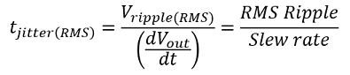
When the gate-source and/or source-drain voltages fluctuate, as well as the equivalent RC time constant at the output, it causes the rise time and switching threshold to fluctuate. This fluctuation in the rise/triggering time is called jitter (in digital signals) or phase noise (in analog signals). Typical jitter values are in the neighborhood of 100 ps/mV. To a first-order approximation, jitter can be calculated with the following equation:
The image below shows how jitter affects digital signals. Note that this applies to clock pulses and digital signals produced by ICs. It is important to note that highly stable clocks are more resistant to power fluctuations and should be used in any system where ultra-accurate timing measurements are required.
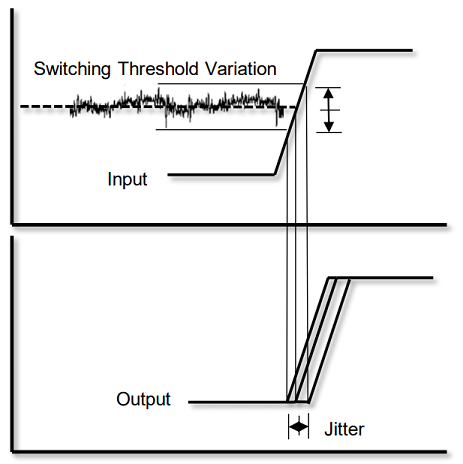
Jitter caused by fluctuations on your PDN
Fluctuations in the Output Signal Level
Power integrity problems also create signal integrity problems by superimposing their noise on the output from an IC. In other words, the output signal from a driven IC can exhibit some noise or droop if there is strong ringing on the PDN. This can cause the signal to fail when attempting to drive a downstream component, either because the signal level is in the undefined region or because it fluctuates between ON/OFF and undefined. Jitter also has a role to play in edge-triggered components. Any noise and jitter on the leading and/or falling edges of a digital signal may cause the gates in a downstream component to trigger incorrectly.
Exploring Tolerances
As supply voltages and signal levels for advanced PLDs and SoCs continue decreasing, the supply tolerances have also decreased. For extremely low power devices, the PDN voltage seen at supply pins is quite low because the transient current pulse they draw has low amplitude and rise time. However, PLDs with high gate count can draw amps-worth of current from the regulator, which can create a large voltage ripple on the PDN. This also places difficulties in measuring and properly quantifying fluctuations, as shown below.
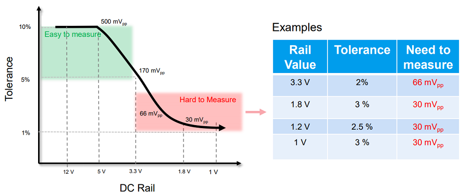
Jitter voltage and PDN impedance tolerances for different supply voltages.
This places greater pressure on designers to properly design and simulate their PDN. The goal in PDN design is to reduce the PDN impedance to as low as possible throughout the relevant bandwidth at which your board will operate, reaching down to milli-Ohm levels in advanced PCBs. This requires significant decoupling in the PDN, which is why power and ground planes should be placed in adjacent layers in your layer stack when working with low-level, high current drawing devices. Decoupling capacitors should also be used to provide a sufficiently large charge reservoir to compensate the transient current draw from your board’s regulator.
Thanks to Jason Ruffing from Rhode & Schwartz for preparing the images that appear in this article.
Originally published at Northwest Engineering Solutions, November 6, 2019.
Have a question about something in this article? You can receive help directly from the article author. Sign up for a free trial to get started.
Comments (0)