Optimizing PCB Trace Width for Low Inductance and Current Requirements

It is often said that one solution to reducing transient ringing in a PCB trace is to simply use wider traces. This is true to an extent; making your traces wider will reduce ringing as it reduces the inductance in a trace, which increases the level of damping seen by a signal traveling on an interconnect. However, changing the trace width also changes the impedance of your trace. While ringing cannot be completely eliminated in a perfectly impedance matched transmission line, it can be reduced to the point where it does not cause overshoot or undershoot in the signal level to put a signal in the receiver’s undefined region. You can figure out the best trace width to use in your board if you reframe your PCB trace width calculation as an optimization problem.
How to Optimize PCB Trace Width
The process of optimizing PCB trace width must meet two objectives:
- Minimized inductance. If you look at the most accurate equations describing trace impedance and inductance, you’ll find that there is a specific width that will produce minimum inductance for a given impedance value and distance to the trace’s ground plane.
- Sufficient current carrying capacity. The current carrying capacity in a PCB is a function of the trace geometry and the desired temperature rise. This can be determined from the IPC 2152 nomograph.
If you need to determine the trace width that produces minimum inductance for a given desired impedance value, then you need to start with the right trace impedance equations. Let’s take a look at how to do this for microstrips. Note that the process I’ll present here can be easily adapted to striplines, coplanar waveguides, or any other trace geometry.
Example: PCB Trace Width for Microstrips
Hartley’s equations are widely regarded as the most accurate equations for describing trace impedance for a broad range of geometries. The IPC 2141 equations are only accurate within a certain impedance/trace geometry range, as was shown in a 1999 study by Polar Instruments. Eq. (1) shows Hartley’s equations for the impedance of a microstrip:
Eq. (1): Microstrip impedance from Hartley’s equations.
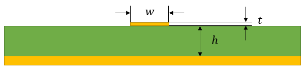
Fig. 1: Microstrip trace geometry used in Eq. (1).
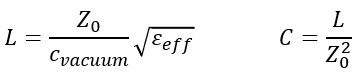
One can easily determine the inductance and capacitance from the propagation delay and impedance equations, assuming the transmission line is lossless, and there is no dispersion:
Eq. (2): Lossless microstrip inductance and capacitance.
This system is self-consistent in that you only need to input the value of the dielectric constant at your desired frequency. Here, we are only considering an isolated single-ended transmission line, meaning there is no coupling to other traces through parasitic inductance or capacitance. Obviously, this does not represent the true situation in a real PCB, but it is a good place to start when determining the right PCB trace width you should use to suppress transient ringing and impedance matching in a transmission line.
Determining the PCB trace width you need to minimize inductance while controlling impedance to a specific value is a difficult problem to solve analytically or graphically. Here, you have three variables to optimize, which are h, w, and t. In a real board, the layer thickness depends on the prepreg and core thicknesses, so you are generally constrained to different possible values of h. This means you can reduce the number of relevant variables to the ratios (t/h) and (w/h). In other words, for a given value of h, you now know the values of w and t as long as you know the ratios (w/h) and (t/h), respectively.
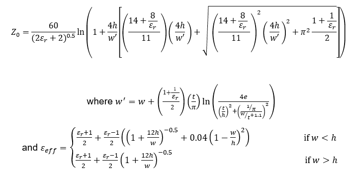
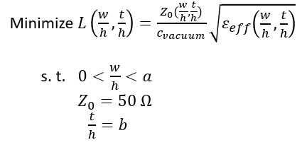
The effect of changes in these variables is shown in the graph in Fig. 1. If you want to determine the value of (w/h) that minimizes inductance for a given value of (h), then you need to construct multiple graphs and determine intersections at the desired trace impedance value. This is very time-consuming and prone to errors. The alternative is to calculate critical points from derivatives, but you will then need to solve products of piecewise transcendental equations, which will have multiple numerical solutions.
Fig. 1: Microstrip impedance and inductance as a function of PCB trace width to height ratio.
PCB Trace Width as an Optimization Problem
The better option is to frame Eqs. (1) and (2) as an optimization problem with (t/h) set to a specific value. Note that you could take (t/h) as an optimization variable, but this may produce infeasible results. Because (t) is determined from the copper weight in your board, and (h) is determined from the prepreg or core thickness, it is better to define (t/h) as a constraint. This optimization problem would be defined as follows:
Eq. (3): Defining PCB trace width as an optimization problem.
This optimization problem can be easily solved using an iterative numerical algorithm, such as an evolutionary algorithm or reduced gradient algorithm. This is better than using a semi-numerical method such as Kuhn-Tucker as you will still have the problem of solving transcendental equations for the trace geometry. For a set of free evolutionary optimization algorithms that can be immediately brought into Python, take a look at Sky Workflows. For now, I’m going to just use the Solver in Excel, which includes an evolutionary algorithm.
Results: 1.0 oz./sq. ft. Copper Weight, 6-layer FR4 Board
The results below show an example for a 6-layer board with a total thickness of 1.57 mm. I’ve taken a simple situation where the board is divided into 6 equal-sized layers, giving h = 0.262 mm. Using 1.0 oz./sq. ft. copper weight gives t = 0.035 mm. To solve this problem, I’ve set the upper limit on the search space in Eq. (3) to a = 5. Finally, my desired impedance is Z = 50 Ohms, and I’ve used a dielectric constant of 4. My optimization results are shown in Fig. 2.
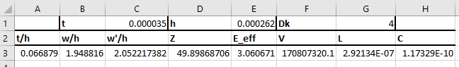
Fig. 2: PCB trace width results, giving (w/h) = 1.949 for a desired impedance of 50 Ohms.
This procedure produces the result (w/h) = 1.949. With t = 0.035 mm, we have a PCB trace width of w = 0.510 mm, or 20 mils, and the minimum inductance is 292 nH/m. For a 1 inch trace, this value would have a total inductance of ~7.5 nH, which is consistent with typical trace inductance values. You can then check this PCB trace width against the IPC 2152 nomograph to determine the maximum current carrying capacity and possible temperature rise.
Going Further: Including Losses and Dispersion
The above method works perfectly for transmission lines that are running at a sufficiently high frequency that resistive losses can be ignored. Dispersion can be ignored when the transmission line is used with analog signals as you are only working at a single frequency, and you can use the Dk value for that particular frequency. With digital signals, the signal bandwidth can span more than a decade, and you need to know the dielectric constant as a function of frequency. This is important for properly describing causal behavior in any transmission line.
UPDATE: I've put together an IEEE paper that includes dispersion in this model and accounts for resistive losses as part of the optimization process. I'll provide more updates on this and will be presenting this work at the IEEE WMED 2020 conference.
Sizing your PCB trace width in controlled impedance routing can be difficult, so working with an experienced design firm can be a huge help.
Ed: To learn more about the author, please visit his Experts Exchange Profile Page.
Have a question about something in this article? You can receive help directly from the article author. Sign up for a free trial to get started.
Comments (0)