
What is Transmission Line Dispersion?
Dispersion is a fundamental property of the interaction between real materials and the electromagnetic field. This physical property refers to the fact that the real part of a material’s dielectric function, and thus the speed of an electromagnetic wave, is a function of the wave’s frequency. In addition to the real part of the refractive index, the imaginary part of the dielectric function is also a function of the wave’s frequency. This explains why different materials absorb and transmit different colors of light.
Modeling dispersion on a transmission line requires accounting for the dielectric properties of the substrate and bringing them into a model for the line’s characteristics impedance. Once you’ve included these values in the line’s impedance, you can calculate the equivalent parameters in the RLCG(f) model as functions of frequency, and you can calculate losses on the line as a function of frequency.
Dispersion and Losses in Transmission Line Characteristic Impedance
The standard model for calculating transmission line impedance is the RLCG(f) model, where the transmission line is modeled using the circuit parameters shown below. The characteristic impedance can be calculated in terms of the equivalent circuit parameters using the Telegrapher’s equations.
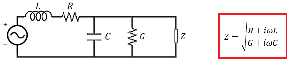
RLCG(f) model for transmission line impedance without dispersion and skin effect losses.
Most designers that use this model do not include dispersion in the calculations. In other words, they simple assume that, at high frequency, the dielectric constant does not change and the transmission line's characteristic impedance converges to a purely resistive value:
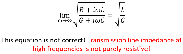
RLCG(f) model transmission line impedance approximation.
This is simply not correct. I’ve seen a prominent manufacturer that uses this equation for controlled with baseband chips, which is not correct. Here’s why this approximation is incorrect:
- C and G are functions of frequency. Both of these terms are functions of frequency as they depend on the dielectric constant (real and imaginary parts, respectively).
- The skin effect is ignored. The skin effect adds some resistance to the line in addition to the native DC resistance of the conductor. The skin effect also adds some reactive impedance to the line as it creates eddy magnetic fields, thus it adds a frequency-dependent contribution to L.
In reality, the impedance of a transmission line has a reactive component. While this reactive component is small, it is not zero at high frequencies and it contributes to signal deformation. Furthermore, the skin effect resistance and the conductive losses depend on the geometry of the trace. Calculating this behavior throughout the signal bandwidth correctly requires considering the causal nature of the electromagnetic field and how it manifests as signal behavior on a transmission line. In this case, this requires defining the real and imaginary parts of the dielectric function using Kramers-Kronig relations (see below). The correct parameters in the RLCG(f) model and their relationship to the frequency-dependent dielectric function are shown below.
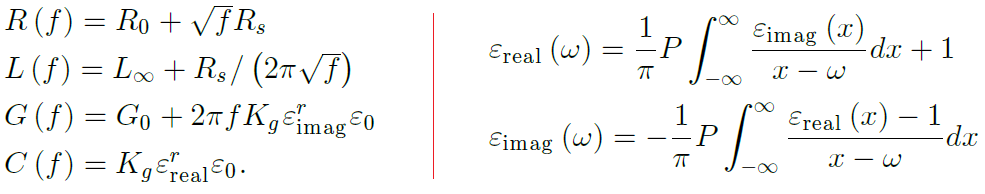
(Left) Frequency-dependent parameters in the RLCG(f) model describing causal transmission lines, including transmission line dispersion, DC losses, dielectric losses, and the skin effect. (Right) Kramers-Kronig relations between the real and imaginary parts of the dielectric function.
Source: J. Zhang, J. L. Drewniak, D. J. Pommerenke, M. Y. Koledintseva, R. E. DuBroff, W. Cheng, Z. Yang, Q. B. Chen, A. Orlandi, "Causal RLGC(f) Models for Transmission Lines From Measured S-Parameters," IEEE Trans. Electromagn. Compat., vol. 52, no. 1, pp. 189-198, Feb. 2010.
Effects of Dispersion and Losses on Impedance and Insertion Loss
The typical practice of simply reducing to the standard resistive formula for the characteristic impedance of a transmission line is clearly incorrect, as can be seen in the above equations. The typical resistive formula is only an approximation that is generally valid below ~10 GHz. Instead, the actual impedance is a complex function of frequency, as shown in the graphs below. Similarly, the traditional resistive formula underestimates insertion loss, forcing designers to apply pre-compensation at the source end of the line.
The graphs below show some results for the characteristic impedance and insertion loss in a stripline on FR4. This calculation includes the skin effect losses and dispersion in the dielectric. We can see that this optimized transmission line geometry provides low loss out to 20 GHz, and the loss is somewhat lower than other stripline designs I’ve seen. We can see that the impedance is not purely resistive. This stripline has copper weight of 1 oz./sq. ft., 0.196 mm layer thickness, and 0.54 mm width (21.3 mil).
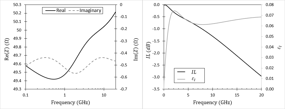
(Left) Characteristic impedance, and (Right) Insertion loss and imaginary part of the dielectric function in the designed stripline with optimized geometry.
This line was designed while accounting for transmission line dispersion, DC losses, dielectric losses, and the skin effect, and by using the causal relations for the dielectric function. You can read more about the procedure for optimizing the geometry of a transmission line using conformal mapping results in this article. This was done without the use of simulations or direct calculation of parasitics in the transmission line.
Managing Transmission Line Dispersion
Finding a balance between transmission line dispersion, losses, and impedance variations/deviations is not such an easy task if you look at the typical models for PCB design. Most design firms and manufacturers don’t understand the effects of transmission line dispersion, and they get the math and physics just plain wrong. Most designers who use transmission line impedance models for impedance control get it wrong in the following ways:
- They don’t use experimental data for the dielectric function. Most designers will simply assume a specific value for dielectric constant, and they often do this at the incorrect frequency. While a single value for the dielectric constant might be fine for a harmonic signal, it’s simply wrong when working with a digital signal, especially at fast rise time.
- They don’t know how to calculate a transmission line’s impedance spectrum. I’ve never personally met a designer that knows how to do this correctly. However, I know some designers that understand the importance of calculating the impedance spectrum throughout the bandwidth; they usually do this using a finite-difference frequency-domain (FDFD) post-layout simulation. However, you can do this analytically without using field solvers.
Dispersion and losses are unavoidable, and you need to work with a design firm that understands how these factors are related to the geometry of your board and traces. I’ve spent a significant amount of time working on developing the optimization procedure for designing transmission line geometries for use in controlled impedance routing. This was used to create the graphs shown above. As I’ve built out this procedure, the current incarnation of the model incorporates transmission line dispersion, losses, distortion, and the skin effect throughout the signal bandwidth. A paper with these results is currently under review with IEEE, and I anticipate I’ll be asked to present these results at AltiumLive 2020. This type of procedure is the best way to see the tradeoffs between dispersion and losses, as well as how to link these important transmission line properties back to transmission line geometry.
Note: Controlled impedance routing for digital signals with ~20 GHz bandwidth requires a meticulous design process and you need a good design firm to build these systems.
Have a question about something in this article? You can receive help directly from the article author. Sign up for a free trial to get started.
Comments (0)