
Simply put, the geometry of your traces, signal frequency content, and layer arrangement will determine your PCB return current path. The signal itself will, in some ways, choose its own return path. However, with some basic design guidelines, you can ensure the return current does not pass through a region where it could cause interference in other circuits. Once a designer understands how signal characteristics influence the return path, it becomes easier to design an intended return path for signals without resorting to electromagnetic field solvers.
PCB Return Current Paths at Different Frequencies
A PCB return current path is determined by the impedance between a signal trace and the impedance of the circuit that carries the return current. Current in a PCB flows from the power supply, to downstream components, and from outputs to further downstream components. Along the way, current is induced in the reference plane and propagates back to the ground return point.
We like to think that current ‘flows’ along this circular path, although this is not really correct. This picture of flowing electrons is convenient for visualizing the distribution of current in a PCB, but it leads to incorrect explanations of circuit behavior; a prime example is in right-angled PCB traces. In reality, the return current for a propagating signal depends on the frequency and associated impedance seen by the signal as the electromagnetic field propagates along an interconnect.
- DC current. With DC current, the return current path is simply the path of least resistance. This means the current follows a straight line from the source and back to the ground return point. This means the DC current in the ground plane just follows a straight line back to the power supply.
- Low frequencies. At low frequencies, a portion of the return current path follows beneath the trace carrying the signal. The current is spread around the trace in a Gaussian-like distribution.
- High frequencies. At high frequencies, the return current path closely follows the path beneath the trace.
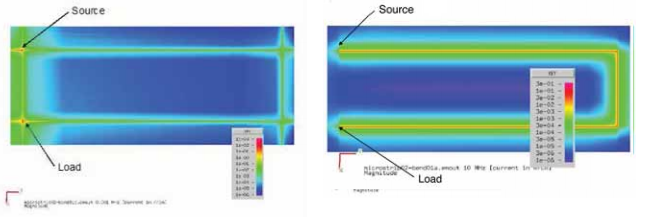
Return path as a function of frequency. Left: 1 kHz, Right: 1 MHz. These images can be found in Resistive vs. Inductive Return Current Paths by Bruce Archambeault. You can read more about the influence of parasitics in your PCB in this article.
Inductive vs. Capacitive PCB Return Current Path
Why is there a difference in PCB return current path behavior? If you remember your electronics 101 class for a moment, the impedance of a circuit can be split into resistive (independent of frequency) and reactive (dependent on frequency) contributions. In reality, real circuits on a board should be modeled, at minimum, as RLC circuits; this is the standard approach with transmission lines. This is the case for any circuit, even if said circuit does not contain capacitors or inductors.
Because conductors are separated from their ground return path by an insulating substrate, there is always some parasitic capacitance. Parasitic inductance arises because all circuits form a closed loop of conductive material. These parasitics and the natural DC resistance of conductors contribute to the impedance seen by signals as they travel throughout your board. This means the path the return current must travel in a real board will have some capacitive and inductive contribution in series with a resistive contribution.
Low Frequencies = Inductive Return Current Path
The return current will only follow directly below a trace at all frequencies, as was mentioned above. At low frequencies, the return current is inductively induced in a loop surrounding the circuit. This creates the apparent straight-line path at low frequencies shown in the above figure (left panel). In reality, there is a current loop beneath the trace that extends throughout the reference plane.
High Frequencies = Capacitive Return Current Path
In contrast, at sufficiently high frequencies, the capacitive nature of the PCB return current path will dominate. This is because there is stray capacitance between a trace and all nearby reference planes. The closest reference plane will have the highest parasitic capacitance and thus the lowest impedance. Therefore, the majority of the return current will be induced as a displacement current in the nearest reference plane at higher frequencies.
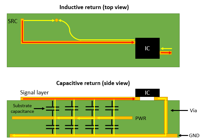
Inductive and capacitive PCB current return paths.
Designing a PCB Return Current Path
The return current path in a PCB is not something to be deliberately designed at every frequency. Instead, some simple stackup and layout choices will determine whether you can properly direct the return path in your PCB such that there is no interference between signals.
Use Adjacent Reference Planes
If you look at the examples with inductive and capacitive return paths above, you’ll see that the use of an adjacent ground plane is the best way to provide a predictable return path. Otherwise, your signals will try to couple inductively or capacitively back to the nearest return plane. This then can cause interference as the return current path establishes itself between power, signal, and finally ground layers. Instead, provide an adjacent ground plane for return signals to prevent unintended coupling.
Mixed Signals and Layer Transitions
For mixed signal boards, the best way to plan the return path is to define analog and digital sections in your board. It doesn’t matter if you use different ground planes, and I advocate using a single ground plane to define return currents. If you use separate ground planes (e.g., one analog, one digital), the two planes will still couple capacitively, allowing analog and digital signals to co-mingle in each other’s ground layers. You would still have to section your board into analog and digital portions to prevent any interference.
When I say "section," I am not talking about cutting a ground layer into two pieces and then routing signals over the gap (don’t do this!!!!). I simply mean arrange analog components with each other in one region of the board, and arrange the digital components together in another region of the board. The goal is to prevent the digital signals from travelling beneath the analog region and causing interference.
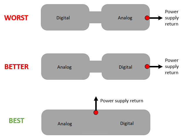
Smart floorplanning can prevent interference between analog and digital sections of your board.
In the case of a layer transition, the best way to ensure a stable return path with low loop inductance is to place a grounded via alongside the signal via. This is the best way to ensure the loop inductance remains small when routing between layers. If you do not do this, the return current will be provided by the nearest decoupling capacitor, which can create very large loop inductance for the circuit in question.
Have a question about something in this article? You can receive help directly from the article author. Sign up for a free trial to get started.
Comments (0)