
Just as Moore's Law has brought transistor gate sizes to ever smaller dimensions, PCBs have followed suit. Although HDI layout is not a new technique, it is critical in many systems that have high component count and high net count. These boards have enabled many new products, such as new smartphones, powerful custom computers (such as those we build for our customers), networking equipment, and much more.
Designers don't normally plan to create an HDI layout unless they are working with specific components that require such layout and routing techniques. On the contrary, they are often forced to work in the HDI regime for a number of reasons. If you suspect you'll need to work with component densities that require HDI layout and routing, here's what you need to know about your next board and how to plan your design.
What is an HDI Layout?
High density interconnect (HDI) layout refers to a set of techniques used to layout a PCB when traces widths generally drop below 8 mils (0.2 mm). These techniques are designed to ensure you can fit a higher density of components onto a single board, allowing you to keep your board size small while increasing component count. Not all boards need HDI layout techniques for a number of reasons, while some components require HDI techniques for proper routing.
An HDI board requires smaller vias to make layer transitions, particularly in fine-pitch BGA components and more traces per sq. mm. In order to accommodate fine-pitch components, you'll find the following typical features in an HDI layout:
- Smaller vias: HDI boards use microvias (mechanically or laser drilled), blind/buried, and staggered vias for layer transitions. These vias have smaller aspect ratios than typical through-hole vias. In order to use these vias with finer pitch components, their diameters are smaller, which then limits their useful depth.
- Thinner traces: The thinner traces used in HDI boards are required to make connections to vias on each layer, as well as to in-oad vias. The thinner traces also allow higher trace density, thus the term HDI.
- Higher layer count: We've built non-HDI boards with high layer counts, but HDI board layer counts can easily reach 20 or more layers when working with high pin density components (e.g., FPGAs).
- Lower signal levels: HDI boards are not used for high voltage or high current. This is because the high field strength between neighboring lines will cause ESD, and high currents will cause excessive temperature rise in conductors.
If you look at the above points and the IPC standards, you can figure out when a board makes the transition to the HDI regime, thus requiring HDI layout and routing techniques. According to the IPC-2221A/IPC-2222 standards, the maximum recommended aspect ratio for through-hole vias is 8:1 (aspect ratio = via depth/via diameter). This means, for a standard thickness 1.57 mm PCB, the minimum drill diameter for a through-hole via is 0.196 mm, or ~8 mils. If your vias need to be smaller to accommodate fine-pitch components, then you'll need to use some HDI-specific via designs and thinner traces.

Trace Sizes and Vias in Your HDI Layout
Clearly, the need accommodate fine pitch components or simply a higher density of components is what motivates the need for HDI designs. Traces are fabricated in the same manner as traces on any other PCB, although care is taken to prevent over-etching. Vias are a different beast and may require laser drilling (for low aspect ratios) through a single layer, known as blind or buried vias.
If you need to span multiple layers in an HDI board, you can't use a through-hole via anymore and still comply with IPC standards. For larger diameter microvias, some manufacturers has experience fabricating blind vias that span multiple layers, but this is not common. Furthermore, placing this in your design will likely violate your manufacturer's DFM rules and will cause your board to receive no-bid status. Instead, vias can be placed in individual layers and stacked on top of each other (e.g., stacked microvias or blind-buried vias). The various microvia configurations are shown below.
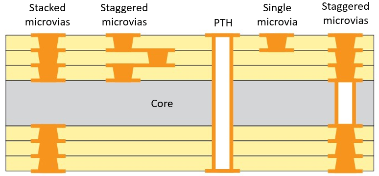
Microvia configurations in a typical HDI layout.
These different via configurations are primarily targeted at BGA components with different pitch. Once your BGA pitch gets to 0.8 mm, you'll likely be able to use a dog bone fanout with in-pad microvias. At 0.75 mm and less, you're better off using plated in-pad microvias (VIPPO) to reach inner signal layers, although you can also route signals between BGA pads to reach the outer pad section during fanout. At much lower pitch (e.g., 0.5 mm), it is not recommended to route between pads unless your manufacturer can reliably fabricate traces below 4 mils.
Basic HDI Design Guidelines
When working with fine-pitch BGA, and the traces and vias that connect to it, there are some basic guidelines that apply to any HDI layout.
- Always check your manufacturer's capabilities. You should generally do this anyways before planning a new design, but nowhere else is this more important than in HDI design. Not all manufacturers have the same capabilities in this area, and it's best to check with your desired manufacturer before you create an HDI layout that can't be fabricated.
- Keep track of spacing between traces and pads. The same idea applies in 1 mm pitch BGAs, the only point that changes is scaling to microvia sizes. Solder mask clearance values are typically on the same size as your trace width. The solder mask clearance depends on the pad size and your pad pitch.
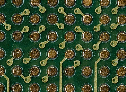
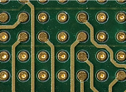
Two HDI layout examples with BGAs. Top: Dog bone fanout with microvias. Bottom: Microvia in-pad.
- Don't use staggered vias or ELIC if you don't need them. The whole point of HDI routing is to provide as much space as possible for routing on the surface and inner layers. While it might be tempting to stack across the entire span of the substrate, don't take up the extra space unless it's really necessary.
- Opt for fewer layers. High layer count boards bring more assembly steps and manufacturing costs. If you follow the previous guideline, you can significantly reduce the cost per board.
- Don't forget about signal integrity when working with HDI boards. Any HDI layout will need to be designed with high speed design guidelines in mind, or high frequency guidelines if you're working with an RF board. The same signal integrity rules that apply in typical PCBs still apply in HDI PCBs, it's just a matter of scaling. In an HDI board that requires impedance controlled routing, you'll need to carefully design your traces and stackup to ensure your impedance is consistent with your signalling standard.
Have a question about something in this article? You can receive help directly from the article author. Sign up for a free trial to get started.
Comments (0)