problem with hi power mosfet failing
Hi I have a PIC18F46K22 MCU and I am using the CPP1 PWM to drive a high power mosfet. The problem I have is very quickly the mosfet remains on and will not switch off.
I have connected the MCU CPP1 pin to a microchip Driver TC1412NEOA this is then connected to a IXFH60N50P3 mosfet NPN type and I have placed a diode SDP30S120 to the positive 330V DC and negative to the drain side of the mosfet. I am only drawing approximately 10 amps when the load is applied to the mosfet I think this is a standard way of connecting these components together and in previous designs using only 12V DC I have had no problem driving a mosfet via the same MCU. Dose anyone have any possible suggestions as to what might be wrong and causing the mosfet to fail and remain on.
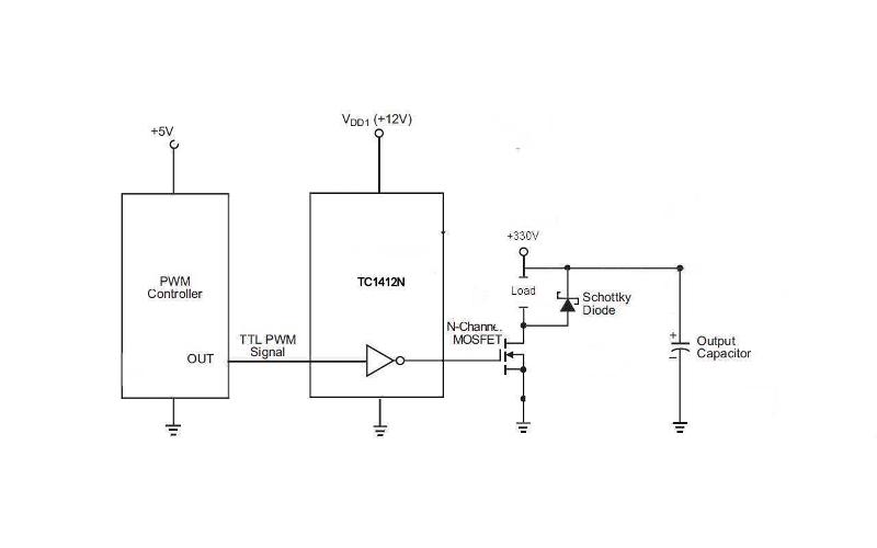
I have connected the MCU CPP1 pin to a microchip Driver TC1412NEOA this is then connected to a IXFH60N50P3 mosfet NPN type and I have placed a diode SDP30S120 to the positive 330V DC and negative to the drain side of the mosfet. I am only drawing approximately 10 amps when the load is applied to the mosfet I think this is a standard way of connecting these components together and in previous designs using only 12V DC I have had no problem driving a mosfet via the same MCU. Dose anyone have any possible suggestions as to what might be wrong and causing the mosfet to fail and remain on.

SOLUTION
membership
This solution is only available to members.
To access this solution, you must be a member of Experts Exchange.
SOLUTION
membership
This solution is only available to members.
To access this solution, you must be a member of Experts Exchange.
Dave Baldwin
In that situation, the MOSFET and the diode should be rated at 1000V to provide adequate margin before breakdown. The TC1412N is rated to drive 1000pf input capacitance in 18ns. Check the input capacitance of your MOSFET. If it is much higher than that, the transistion at the drain will be much slower. That is important because the transition is where all of the power is absorbed by the MOSFET. Also, with that kind of power, a heatsink is a necessity. Even high power devices will not dissipate much power without a heatsink. A device like the NDF10N60Z: Power MOSFET can only handle 39W in free air before it starts to melt.
and it is a good usage to have an insulated coupling between the mosfet and the rest, eg opto coupler
http://en.wikipedia.org/wiki/Opto-isolator
http://en.wikipedia.org/wiki/Opto-isolator
I disagree about the opto coupler. They are usually too slow to drive a MOSFET. A slow transition on a power MOSFET handling that much voltage and current will cause excessive power dissipation and make it more likely that the device will burn out.
ok - fine by me -but how will you isolate the 300V from the rest?
In the situation described, you don't need to. It is only connected to the MOSFET and the load. Circuits like this were common in CRT monitors and TVs. Also in modern switching power supplies although those are driving inductive transformer loads and other restrictions apply there.
ASKER CERTIFIED SOLUTION
membership
This solution is only available to members.
To access this solution, you must be a member of Experts Exchange.
ASKER
Thanks every one for your responses,
I will try and answer everyone to my best ability.
John The Mosfet I am using is capable of continue running at 25 deg @ 60amps according to the specification so I am only inputting approximately 10amps so I am within the specifications of the mosfet. The 12V I was referring to was another design that had a low Gate value which allowed me to drive the mosfet directly via the MCU CCP1 pin max output 5V with a 220R resister between the MCU and mosfet gate.
In this design I am using a much larger Mosfet that uses up to 10V on its gate so I am using a driver to control the mosfet which im thinking might be my problem.
Hi Nobus you have a valid point I think I have covered the isolation issue as I have a 220V AC Primary to 220V AC secondary Transformer 6.6 KVa exactly for this purpose it is then connected to a bridge rectifier which then output 330V DC I use the Mosfet to then control the voltage from 0V to 220V DC via the PWM. But maybe you are referring to the DC side for isolation.
Hi Dave I think you might be onto my issue I have a heat sink on the mosfet and the diode but to be honest the heatsink might be a little small it dose get hot but not that hot that I can't keep my hand on it as I have not successfully been able to run the mosfet for long enough so it hasn't got to hot. I have looked at this PDF http://www.daxia.com/bibis/upload/Matching_MOSFET_Drivers_to_MOSFETs.921.pdf if you take a look at figure 5 this is very much my configuration as I have a ribbon cable connecting between the driver and the mosfet. I also checked the input capacitance of the mosfet 6250pf well over what the driver specs are that im using now. So I have taken a look at another microchip buffer/driver TC4421 and TC4422 it is within the specs of my mosfet. Also in figure 5 of the pdf link provided it suggests placing a zennor diode between the gate and source I was looking to put a 12V rated zennor diode here what are your thoughts on both the TC4421/22 and a 12V zennor diode to over come my issue
Thanks
In this design I am using a much larger MOSFET that uses up to 10V on its gate so I am using a driver to control the MOSFET which I'm thinking might be my problem. <-- This may be an issue.
Also look at the Voltage on the MOSFET to make sure it is within limits. A light load means the MOSFET could see high voltage from the supply line.
then connected to a bridge rectifier which then output 330V DC Did you filter this or do you have high AC ripple on it. 220 V AC is 660 volts peak to peak. So you may have lots of high voltage peaks across the MOSFET.
ASKER
Hi John,
I have a 450V 3600uF Cap on the DC side of the Bridge Rectifier to smoothen out the ripple, I have just ordered some samples of the TC4421A and TC4422A buffer/drivers from Microchip as these chips are designed for high power mosfets im hoping this might resolve my problem but im always open to other ideas and suggestions that others may have and even better some circuits that are proven and work under similar conditions.
I tested the Mosfet by apply 5V to the gate before I connected the PWM and buffer/driver and the mosfet switched on and off ok but it seems when I connected the driver the mosfet refused to switch off and I have a continuous circuit between source and drain even checked continuity between the source and drain and there was a circuit mosfet powered off. So braking down the process off elimination it seems to be pointing to the driver and the capacitance being much to low for the mosfet
Regards
Nigel
The surface between a power device and it's heat sink is a serious thermal barrier even when done completely right. In addition, it takes time for the heat to transfer from the device thru the case to the heatsink. So if the heat builds up too fast, the device will be much hotter than the heat sink when it fails.
For a MOSFET with that much input capacitance, you need a very healthy drive with very good bypassing on the supply rails. When the device switches the input to the MOSFET, there will be a big current spike on the 12V power supply. If the supply voltage doesn't stay up then the drive to the MOSFET is compromised and you will not get the rated switching time but something much slower. That will cause the MOSFET to overheat because it spends much more time in transition.
When the MOSFET is off, you have no power dissipation. When it is all the way on with minimal voltage across it, it may be dissipating less than 10 watts. But right in the middle at 150 volts with 5 Amps (resistive load), it will be dissipating 750 watts. The longer it stays in the middle area, the faster it heats up. If it actually got stuck at 150 volts, you could not cool it well enough or fast enough to save it.